Physical and chemical laboratory equipment:
Mechanical testing, electrical testing, first board inspection and testing, laboratory analysis.
1. Copper foil tensile tester: This instrument is used to measure the tensile strength of copper foil during the stretching process. It helps evaluate the strength and toughness of copper foil to ensure product quality and reliability.
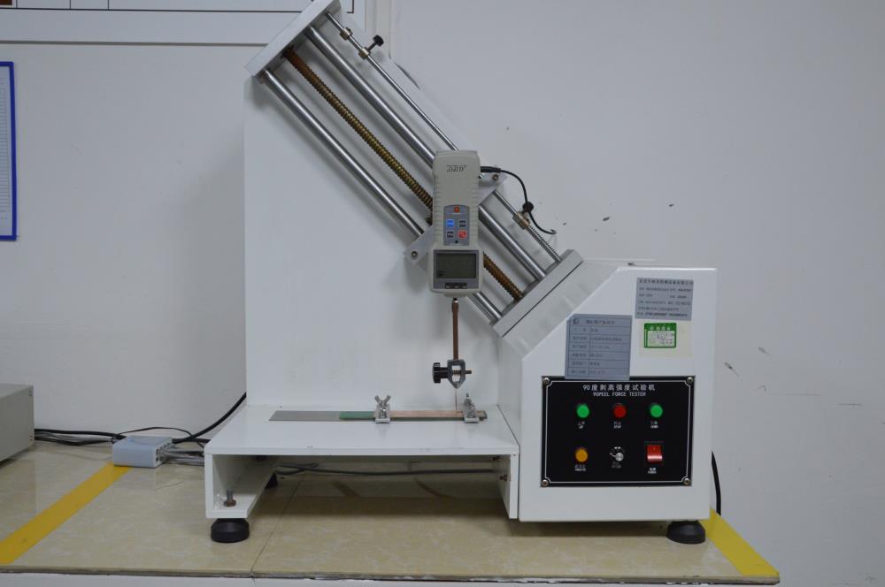
Copper Foil Tensile Tester
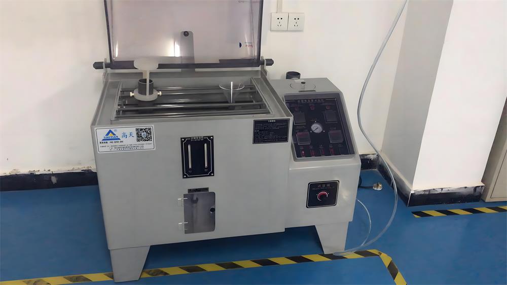
Fully Automatic Intelligent Salt Spray Testing Machine
2. Fully automatic intelligent salt spray testing machine: This machine simulates a salt spray environment to test the corrosion resistance of circuit boards after surface treatment. It helps control the quality of the product and ensure stable performance in harsh environments.
3. Four-wire testing machine: This instrument tests the resistance and conductivity of wires on printed circuit boards. It evaluates the electrical performance of the board, including transmission performance and power consumption, to ensure reliable and stable connections.
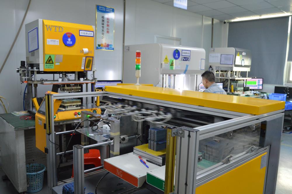
Four-wire Testing Machine
4. Impedance tester: is an essential instrument in printed circuit board manufacturing. It is used to measure the impedance value on the circuit board by generating a fixed-frequency AC signal that passes through the circuit under test. The measurement circuit then calculates the impedance value based on Ohm's law and the characteristics of AC circuits. This ensures that the produced circuit board meets the impedance requirements set by the customer.
Manufacturers can also use this testing process to make process improvements and enhance the impedance control capabilities of circuit boards. This is necessary to meet the demands of high-speed digital signal transmission and radio frequency applications.
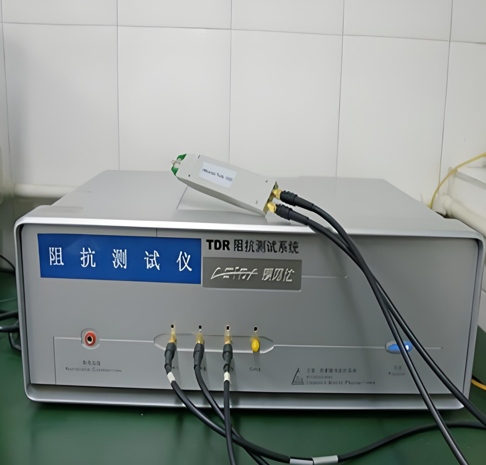
Impedance Tester
Throughout the circuit board production process, impedance testing is conducted at various stages:
1) Design stage: Engineers utilize electromagnetic simulation software to design and layout the circuit board. They pre-calculate and simulate the impedance values to ensure that the design meets specific requirements. This simulation helps assess the impedance of the circuit board before manufacturing.
2) Early stage of manufacturing: During prototype production, impedance testing is performed to verify that the impedance value aligns with expectations. Adjustments to the manufacturing process can be made based on these results.
3) Manufacturing process: In the production of multi-layer circuit boards, impedance testing is conducted at critical nodes to ensure control over parameters such as copper foil thickness, dielectric material thickness, and line width. This guarantees that the final impedance value meets the design requirements.
4) Finished product inspection: After manufacturing, a final impedance test is conducted on the circuit board. This ensures that the controls and adjustments made throughout the manufacturing process effectively meet the design requirements for the impedance value.
5. Low-resistance testing machine: This machine tests the resistance of wires and contact points on the circuit board to ensure they meet design requirements and ensure product quality and performance.
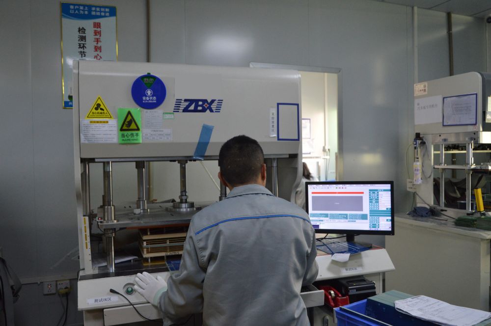
Low-resistance Testing Machine
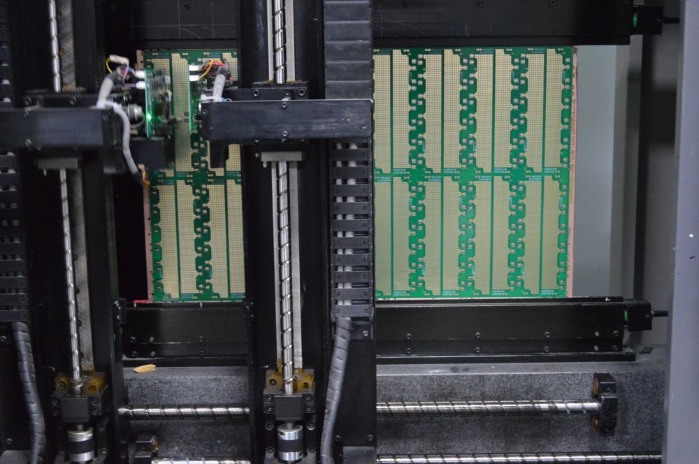
Flying Probe Tester
6. Flying probe tester: The flying probe tester is primarily used to test the insulation and conductivity values of circuit boards. It can monitor the test process and detect fault points in real-time, ensuring accurate testing. Flying probe testing is suitable for small and medium batch circuit board testing, as it eliminates the need for a test fixture, reducing production time and cost.
7. Fixture tooling tester: Similar to flying probe testing, test rack testing is commonly used for medium and large batch circuit board testing. It enables simultaneous testing of multiple test points, significantly improving test efficiency and reducing test time. This enhances the overall productivity of the production line, while ensuring accurate and highly reusable.
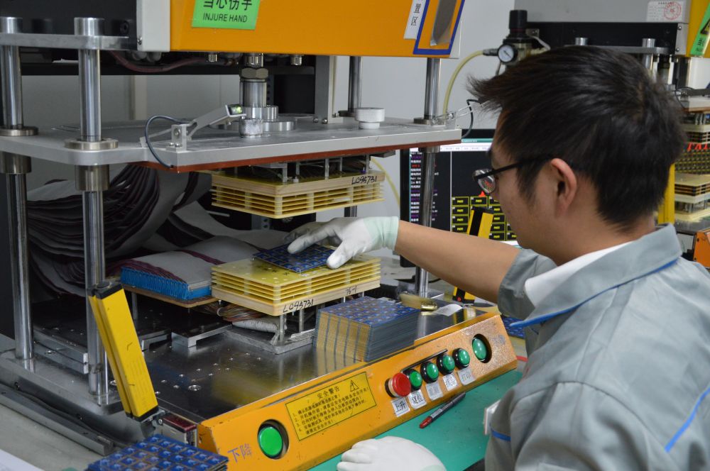
Manual Fixture Tooling Tester
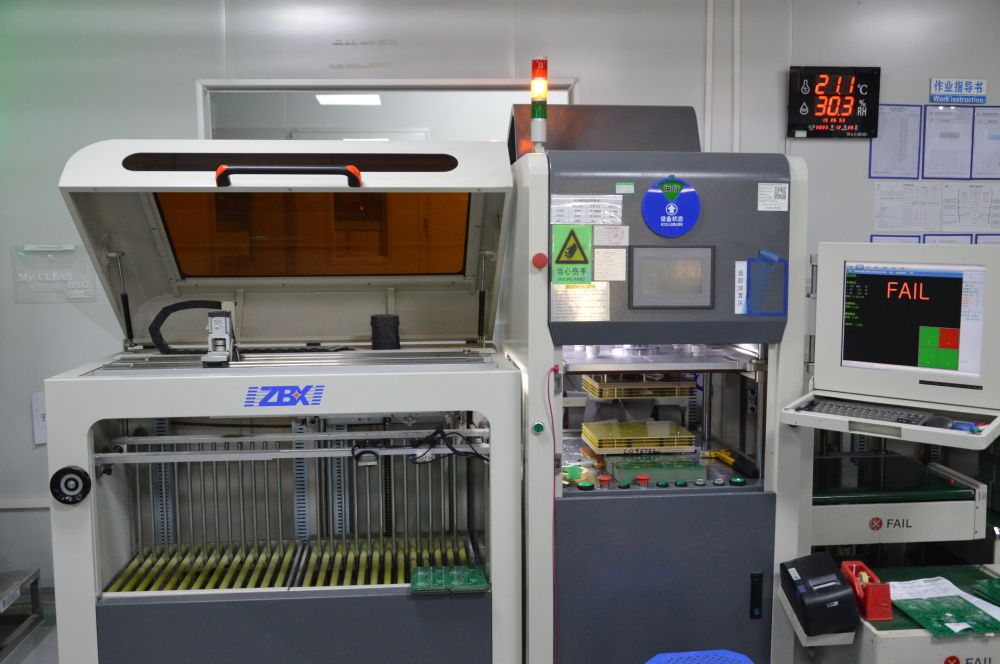
Automatic Fixture Tooling Tester
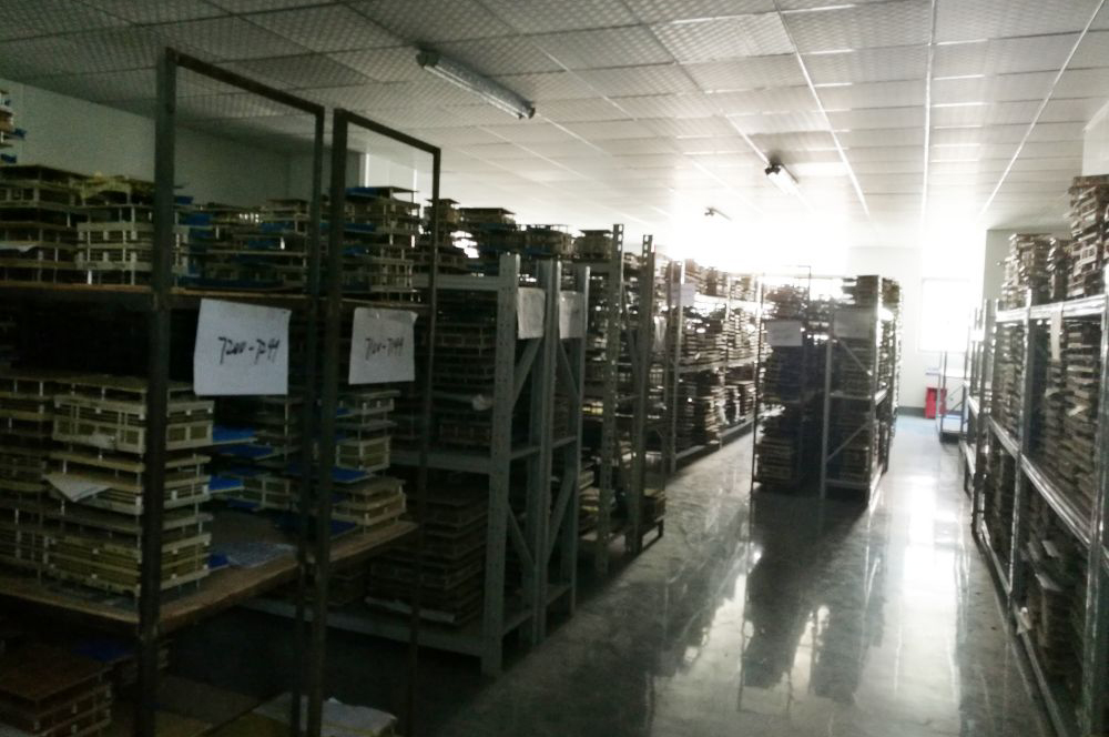
Fixture Toolings Store
8. Two-dimensional measuring instrument: This instrument captures images of an object's surface through illumination and photography. It then processes the images and analyzes the data to obtain geometric information about the object. The results are displayed visually, allowing operators to observe and accurately measure the shape, size, position, and other characteristics of the object.
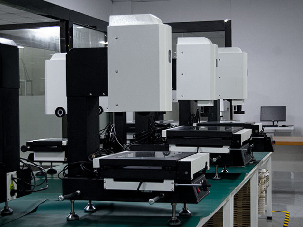
Two-dimensional Measuring Instrument
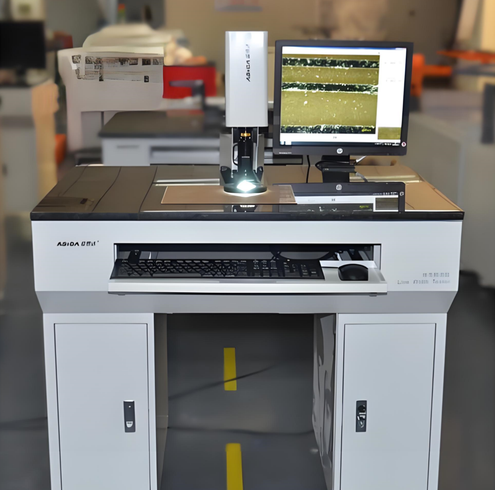
Line Width Measuring Instrument
9. Line width measuring instrument: The line width measuring instrument is primarily used to measure the upper and lower width, area, angle, circle diameter, circle center distance, and other parameters of the printed circuit board's semi-finished products after development and etching (prior to print solder mask ink). It uses a light source to illuminate the circuit board and captures the image signal through optical amplification and CCD photoelectric signal conversion. The measurement results are then displayed on a computer interface, allowing for precise and efficient measurement by clicking on the image.
10. Tin furnace: The tin furnace is employed to test the solderability and thermal shock resistance of circuit boards, ensuring the quality and reliability of solder joints.
Solderability test: This evaluates the ability of the circuit board surface to form reliable solder bonds. It measures the contact points to assess the bonding between the solder material and the circuit board surface.
Thermal shock resistance test: This test assesses the circuit board's resistance to temperature variations in high-temperature environments. It involves exposing the circuit board to high temperatures and rapidly transferring it to lower temperatures to evaluate its thermal shock resistance.
11. X-Ray Inspection Machine: The X-ray inspection machine is capable of penetrating circuit boards without the need for disassembly or causing damage, thereby avoiding potential costs and damage. It can detect defects on the circuit board, including bubble holes, open circuits, short circuits, and faulty lines. The equipment operates independently, automatically loading and unloading materials, detecting, analyzing, and determining abnormalities, and automatically marking and labeling, thereby improving production efficiency.
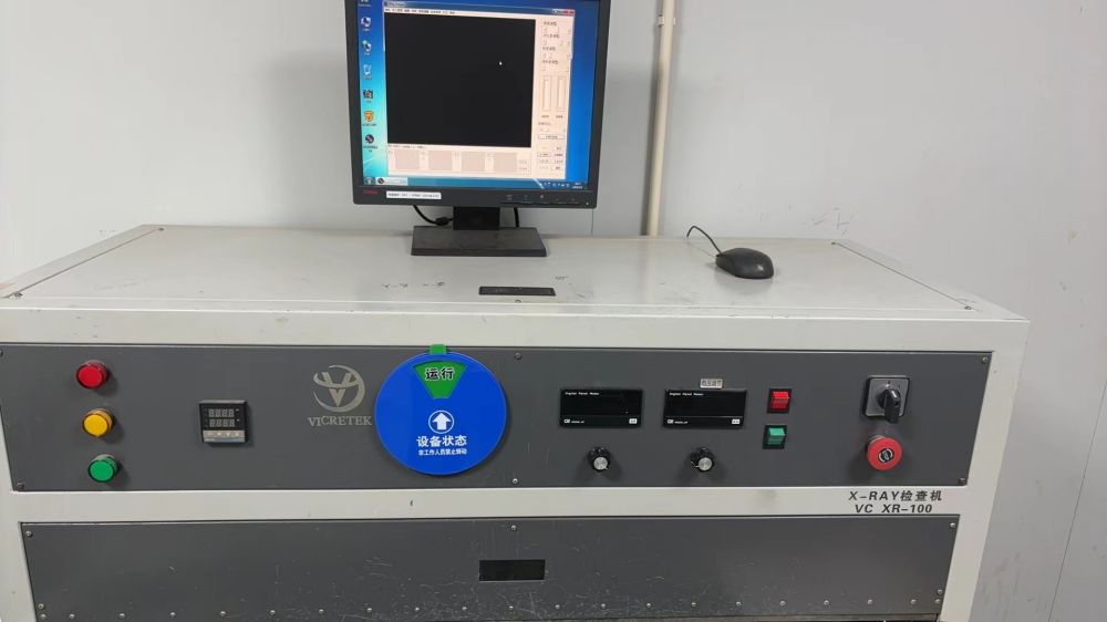
X-Ray Inspection Machine
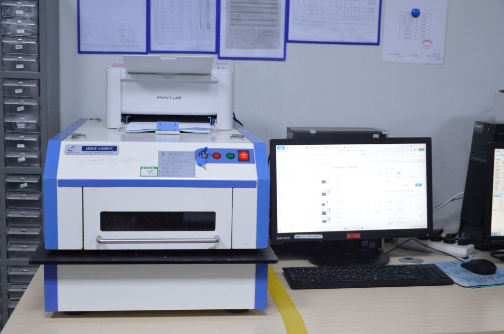
Coating Thickness Gauge
12. Coating thickness gauge: During the manufacturing process of circuit boards, various coatings (such as tin plating, gold plating, etc.) are often applied to enhance conductivity and corrosion resistance. However, improper coating thickness can lead to performance issues. The coating thickness gauge is used to measure the thickness of the coating on the circuit board's surface, ensuring it meets the design requirements.
13. ROHS instrument: In the production of printed circuit boards, ROHS instruments are employed to detect and analyze harmful substances in materials, ensuring compliance with the requirements of the ROHS directive. The ROHS directive, implemented by the European Union, restricts hazardous substances in electronic and electrical equipment, including lead, mercury, cadmium, hexavalent chromium, and others. ROHS instruments are used to measure the content of these harmful substances, ensuring that the materials used in the manufacturing process of printed circuit boards meet the ROHS directive's requirements, ensuring product safety and environmental protection.
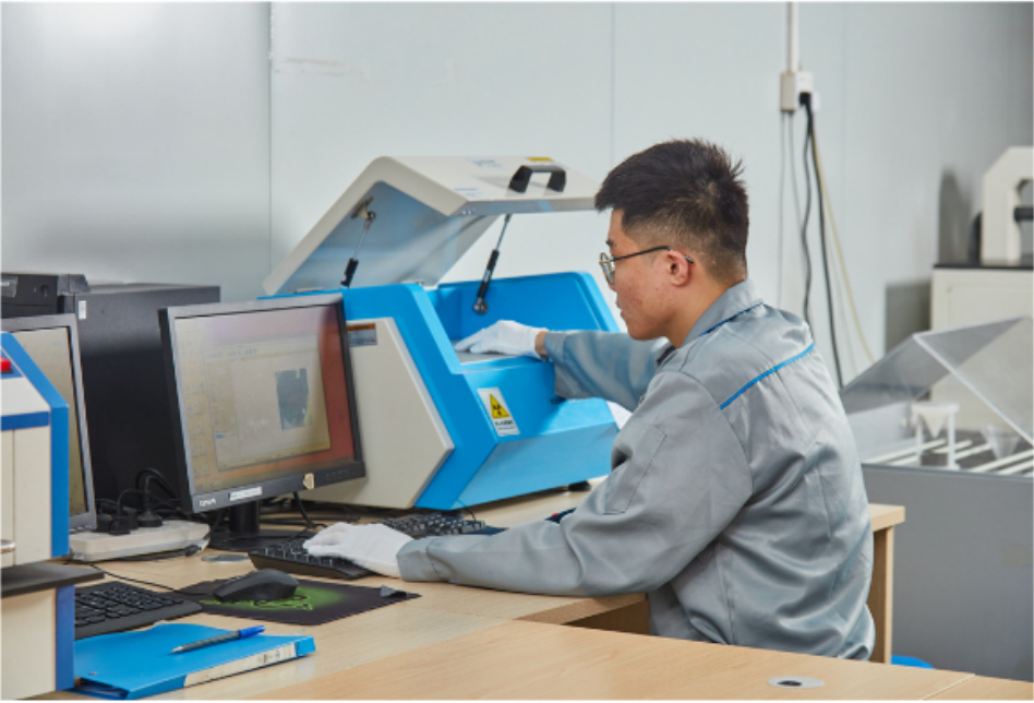
ROHS Instrument
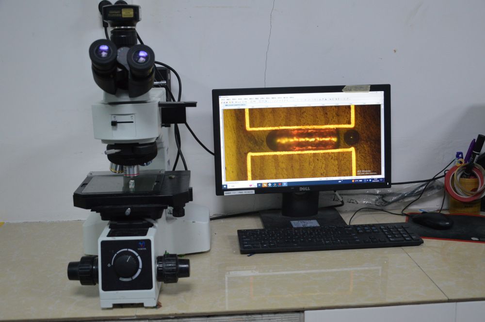
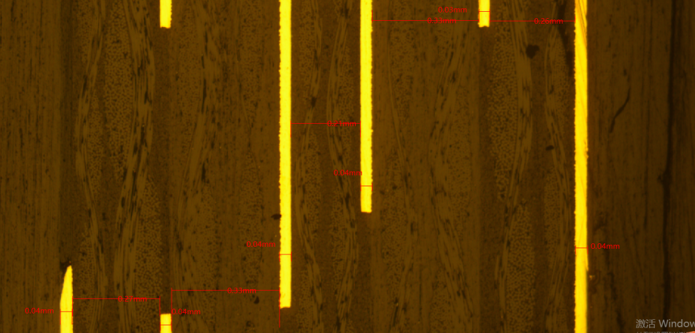
14. Metallographic microscope: The metallographic microscope is primarily used to examine the copper thickness of inner and outer layers, electroplated surfaces, electroplated holes, solder masks, surface treatments, and the thickness of each dielectric layer to meet customer specifications.
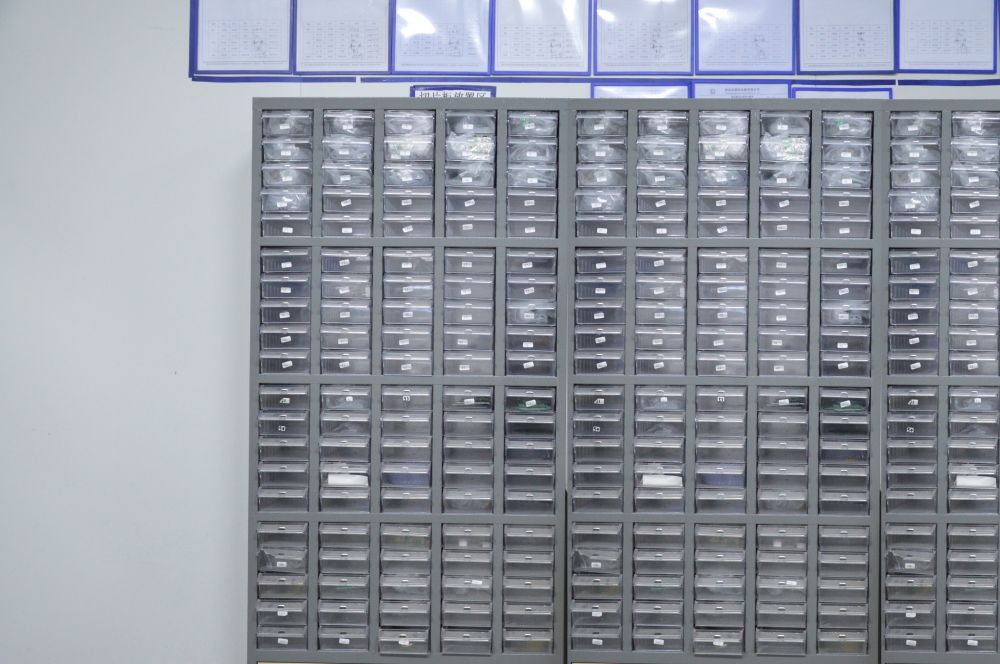
Microscopic Section Store
Microscopic Section 1
Microscopic Section 2
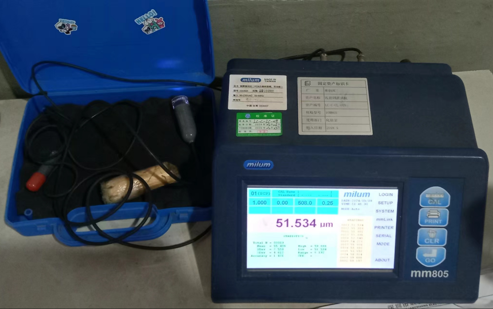
Hole Surface Copper Tester
15. Hole surface copper tester: This instrument is used to test the thickness and uniformity of copper foil in the holes of printed circuit boards. By promptly identifying uneven copper plating thickness or deviations from specified ranges, adjustments can be made to the production process in a timely manner.
16. The AOI Scanner, short for Automated Optical Inspection, is a type of equipment that utilizes optical technology to automatically identify electronic components or products. Its operation involves capturing the surface image of the object under inspection using a high-resolution camera system. Subsequently, computer image processing technology is employed to analyze and compare the image, enabling the detection of surface defects and damage issues on the target object.
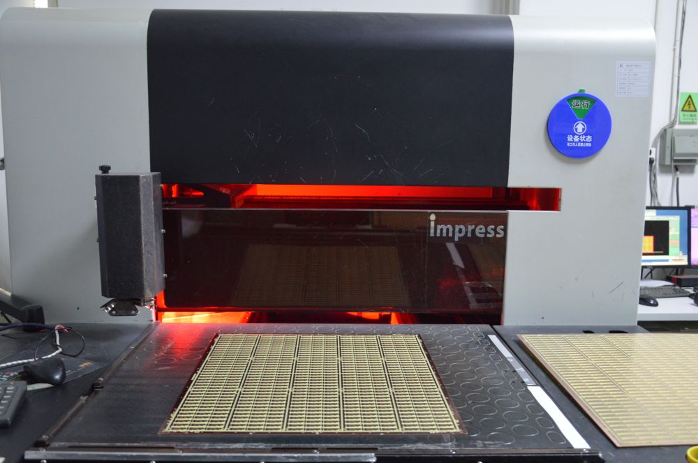
AOI Scanner
17. The PCB appearance inspection machine is a device designed to assess the visual quality of circuit boards and identify manufacturing flaws. This machine features a high resolution camera and light source to conduct a thorough examination of the PCB surface, detecting various defects like scratches, corrosion, contamination, and welding issues. Typically, it includes automatic feeding and unloading systems for managing large PCB batches and segregating approved and rejected boards. By employing image processing algorithms, identified defects are categorized and marked, facilitating easier and more precise repairs or eliminations. Thanks to automation and advanced image processing capabilities, these machines swiftly conduct inspections, bolstering productivity and cutting costs. Furthermore, they can store inspection outcomes and produce detailed reports for quality monitoring and process enhancement, ultimately elevating product quality..
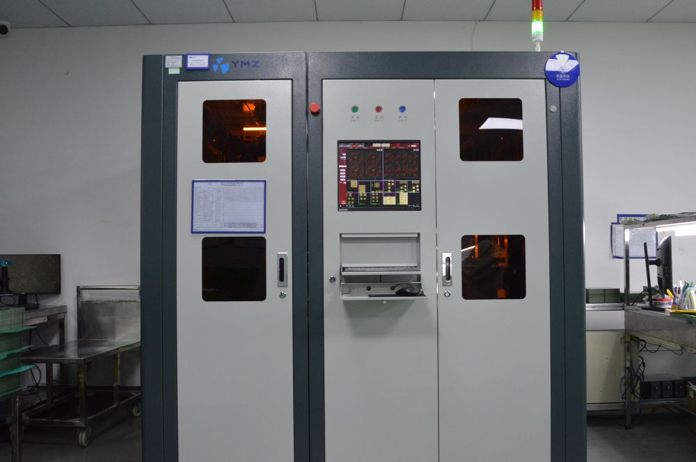
Appearance Inspection Machine 1
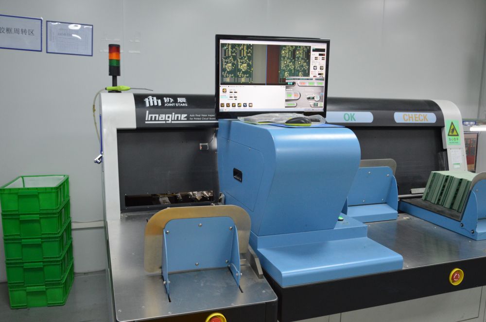
Appearance Inspection Machine 2
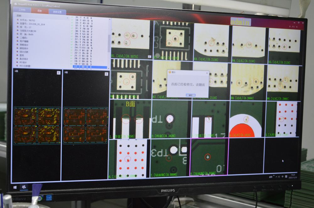
Appearance Inspection Defects Marked
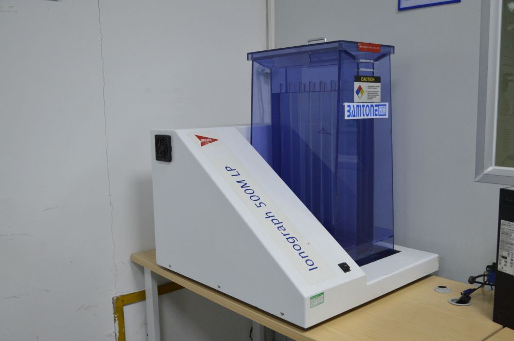
PCB Con Contamination Tester
18. The PCB ion contamination tester is a specialized tool utilized for identifying ion contamination in printed circuit boards (PCBs). During the electronics manufacturing process, the presence of ions on the PCB surface or within the board can significantly impact circuit functionality and product quality. Hence, precise assessment of ion contamination levels on PCBs is crucial to guarantee the quality and dependability of electronic goods.
19. The withstand voltage insulation testing machine is employed to conduct insulation withstand voltage tests to validate that the insulation material and structural layout of the circuit board adhere to standard specifications. This ensures that the circuit board remains insulated under regular operating conditions, preventing potential insulation failures that could lead to hazardous incidents. By analyzing the test outcomes, any underlying issues with the circuit board can be promptly identified, guiding designers in enhancing the board's layout and insulation structure to boost its quality and performance.
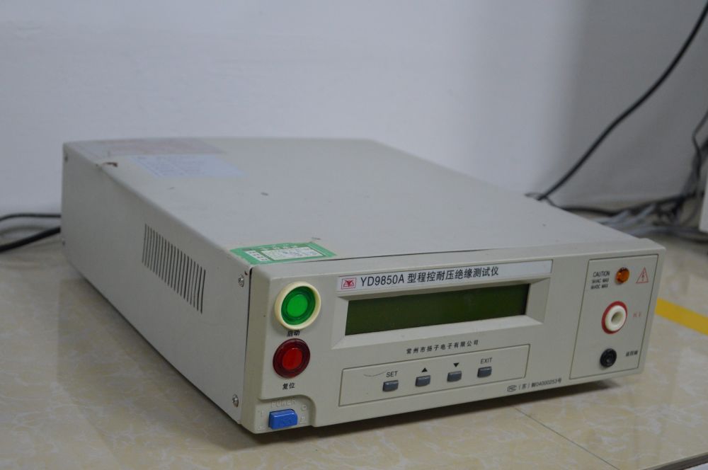
Voltage Insulation Testing Machine
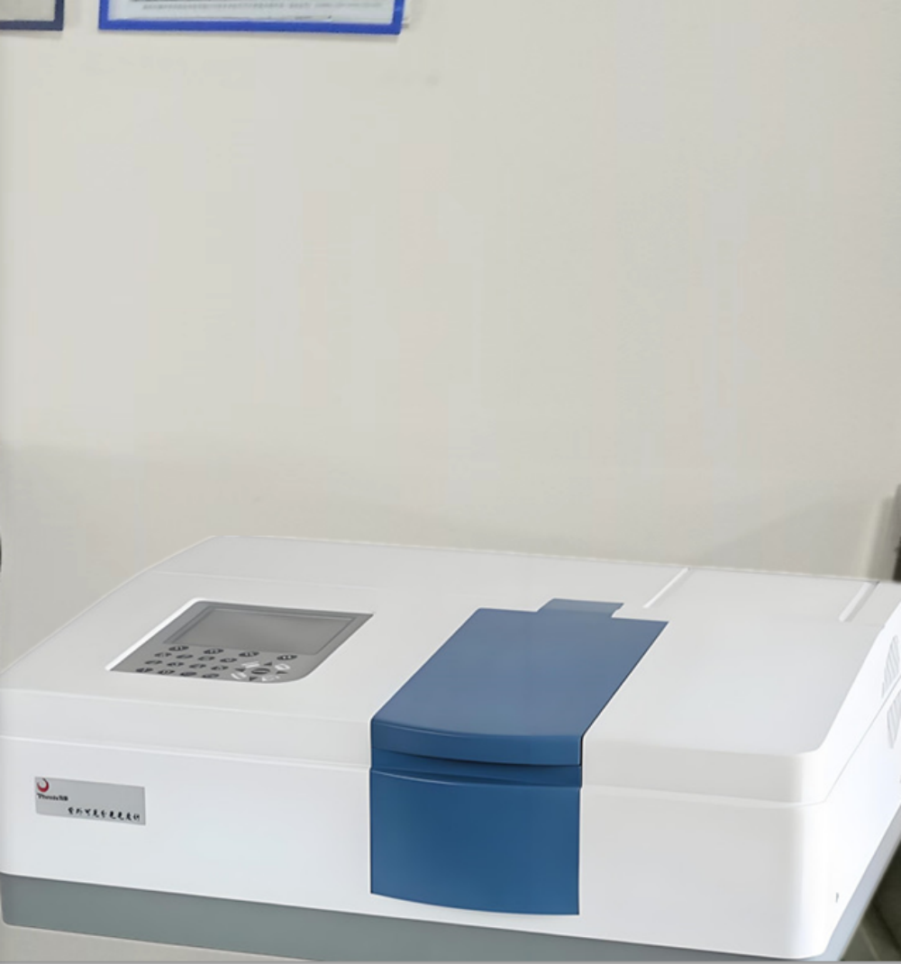
UV Spectrophotometer
20. UV spectrophotometer: The UV spectrophotometer is utilized to measure the light absorption characteristics of photosensitive materials applied to circuit boards. These materials, typically photoresists used in the production of printed circuit boards, are responsible for creating patterns and lines on the boards.
The functions of the UV spectrophotometer include:
1) Measurement of photoresist light absorption characteristics: By analyzing the absorption characteristics of the photoresist in the ultraviolet spectrum range, the degree of ultraviolet light absorption can be determined. This information helps in adjusting the formulation and coating thickness of the photoresist to ensure its performance and stability during photolithography.
2) Determination of photolithography exposure parameters: Through the analysis of the photoresist's light absorption characteristics, the optimal photolithography exposure parameters, such as exposure time and light intensity, can be determined. This ensures accurate replication of patterns and lines onto the photoresist from the circuit board.
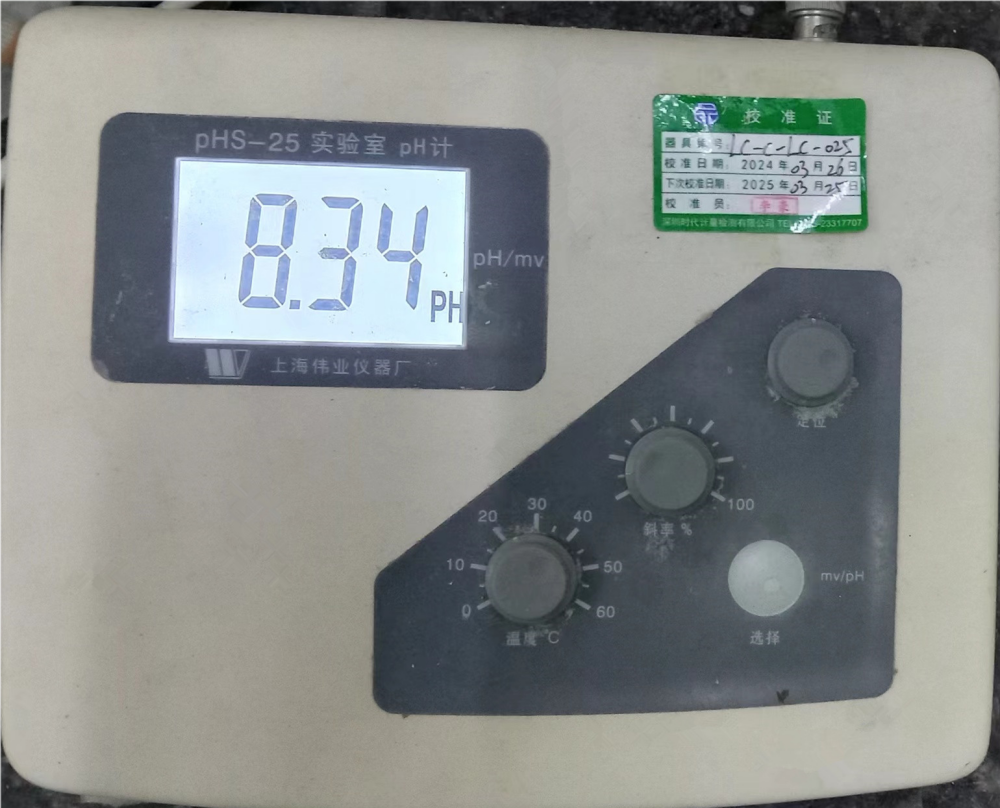
21. pH meter: In the manufacturing process of circuit boards, chemical treatments such as pickling and alkali cleaning are commonly employed. A pH meter is used to ensure that the pH value of the treatment solution remains within the appropriate range. This ensures the effectiveness, performance, and stability of the chemical treatment, thereby improving product quality and reliability while ensuring a safe production environment.
