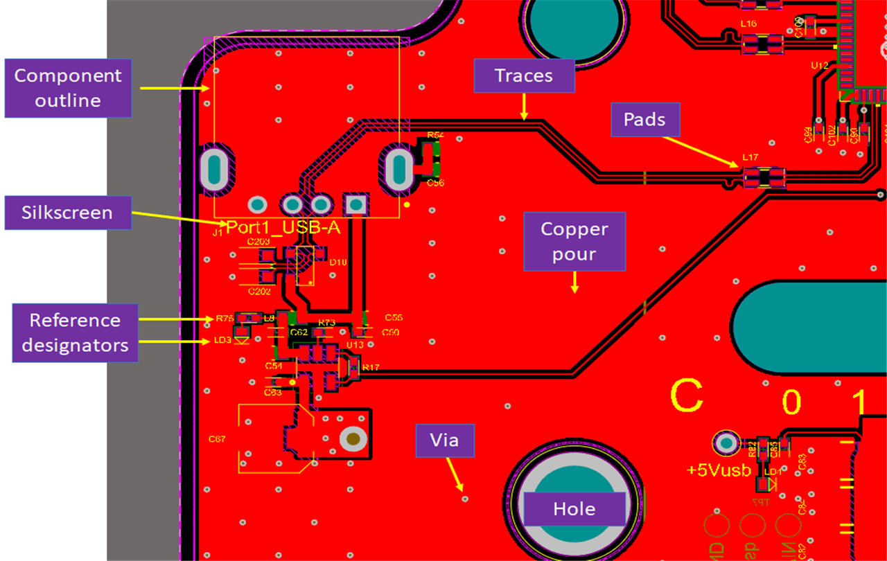
Having a basic understanding of printed circuit board terminology can make working with a PCB manufacturing company much faster and easier. This glossary of circuit board terms will help you understand some of the most common words in the industry. While this isn't an all-inclusive list, it is an excellent resource for your reference.
Being on the same page with your contract manufacturer (CM) is imperative for an accurate embodiment of your design intent to be created without suffering through unnecessary quote delays, redesigns and/or board respins. Precision in communication among all stakeholders in your board’s development is the key.
List of Important PCB Design Terminology

Printed Circuit Board Terminology
Some key printed circuit board terms focus on describing the physical structure of a PCB. These terms are also referenced in design and manufacturing, so it’s important to learn these first.
Layers: All circuit boards are constructed in layers, and the layers are pressed together to form a stackup. Each layer includes etched copper, which forms the conductors on the surface of each layer.
Copper pour: Areas of a PCB that are filled in with large regions of copper. These regions may be oddly-shaped.
Traces and transmission lines: These terms are used interchangeably, particularly for advanced high speed PCBs.
Signal vs. plane layer: A signal layer is intended to only carry electrical signals, but it could also have copper polygons that provide ground or power. Plane layers are intended to be complete planes without any signals.
Vias: These are small drilled holes in a PCB that allow a trace to move between two layers.
Components: Refers to any part that is placed on a PCB, including basic components like resistors, connectors, integrated circuits, and much more. Components can mount by being soldered to the surface (SMD components) or with leads that are soldered into copper holes (through-hole components) on the circuit board.
Pads and holes: Both of these are used to mount components to the circuit board and are used as a location to apply solder.
Silkscreen: This is the text and logos printed on the surface of a PCB. This contains information about component outlines, company logos or part numbers, reference designators, or any other information needed for fabrication, assembly, and regular use.
Reference designators: These tell the designer and assembler which components are placed in different locations on the circuit board. Each component has a reference designator, and these designators can be found in the design files in your ECAD software.
Soldermask: This is the top-most layer in a PCB that gives the circuit board its characteristic color (usually green).
Post time: Feb-14-2023
